
Die bonding is the process of attaching a semiconductor die to substrate/package, providing mechanical robustness, and electrical connectivity and allowing the removal of heat from the device.
Selection of the optimal die attach material and process is based on a number of issues, including thermal requirements, electrical requirements and mechanical stability.
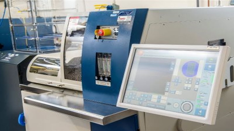
- Epoxy dispense, Daubing or Jetting
- Ag pressure-less sintering paste
- Solder and Eutectic die bonding.
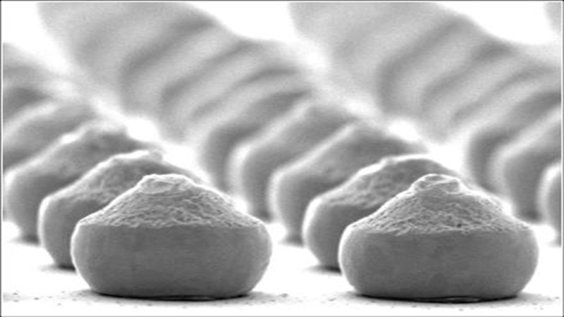
- Placement tolerance down to +/-50um.
Epoxy die attach is a common approach to bonding since it offers the lowest cost and throughput. Epoxies used are generally electrically conductive, or electrically non-conductive. Both material types offer good thermal conduction to remove heat from the chip into the package substrate which can then be further removed through the PCB or specific heat sink.
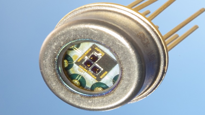
Alter Technology offer epoxy die attach using a needle dispense process, suitable for large die, and an epoxy daubing or stamping process which can create small controlled dots of epoxy for attaching die down to 200x200um such as LEDs and VCSELs.
Epoxies are usually thermally cured during an off-line batch curing process, performing the curing on a batch basis reduces throughput time associated with individual reflow required for solder or eutectic processes.
Ag Sintering
Pressure-less silver sintering pastes are used to offer similar electrical and thermal conductive to solders, but they can be applied and cured in a similar way to epoxy. Alter have used Ag sintering pastes for applications requiring high heat dissipation such as high-brightness LEDs, laser diodes and RF MMIC dies.
Solder Die Attach
ALTER has experience with a wide range of solder materials including soft and hard solders, Pb-free solders, Eutectic solders and solders for operation over a wide temperature range. This knowledge is critical in supporting our customers in making the correct decisions on solder material selection for their product.
For many Optical, MEMS or Sensor devices fluxes can pose reliability concerns with contamination of the sensitive active regions of these devices.
As a result, many of the solder attach processes at ALTER are based on a flux free solder process utilizing solder preforms or pre-tinned substrates with a subsequent Vacuum Reflow process, or reflow using Pulsed Heat-Stages with reducing or cover gas to prevent oxidation.
In order to use a solder attach process, the components require a compatible metal surface. ALTER can provide input on appropriate surface finishes.

Download Datasheets for advanced packaging solutions
Explore our expertise through ALTER’s Packaging and Assembly datasheets. Click now to explore cutting-edge solutions, from fast IC prototype packaging to advanced hermetic sealing. Discover our capabilities in ASIC packaging, MEMS, laser diode modules, and more.


Related services
Hermetic sealing
Plastic encapsulation
Optical alignment
Flip Chip
Wafer sawing
