
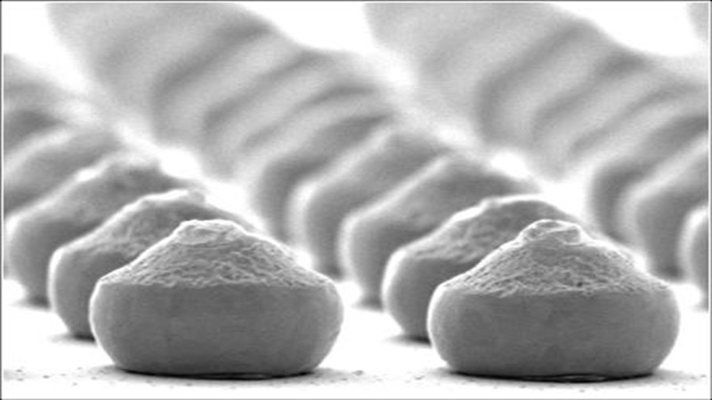
Wafer Sawing is the process of singulating the wafer into individual die ready for subsequent assembly.
ALTER has the capability for dicing wafers and substrate up to 12” in diameter.
- Up to 12” wafers
- Multi-project wafers
- Wide range of process knowledge
- Silicon, SiC, GaN, GaAs, InP, Glass, FR4,
- Sub-dicing of field die

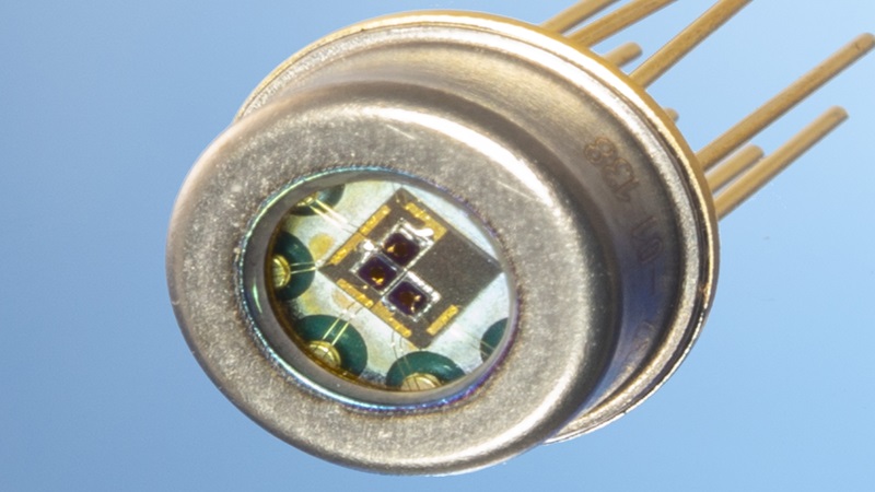
For many Plastic package and System-in-Package (SiP) applications a very thin semiconductor die is required in order to meet the demanding package form factor requirements.
Our engineers have experience of mounting and dicing thin wafers down to 100um in thickness. ALTER can also offer thinning of wafers by using a backgrind process. In addition to handling very thin die our company can also dice substrates up to 1mm thick.
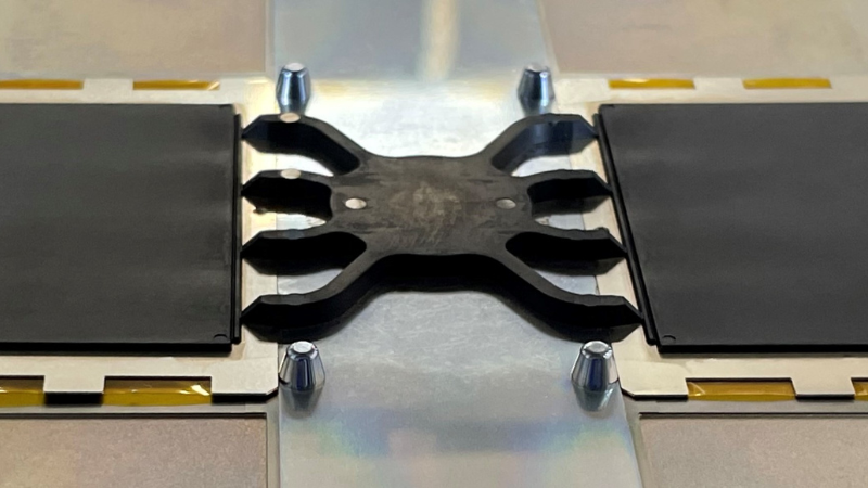
We have an extensive experience in wafer dicing a wide variety of substrates including Si, Multi-Project Wafers (MPW), GaAs, GaN, FR4, Glass, Ceramics and Laminates. Different dicing blade thickness and materials are used depending on the substrate material and thickness.
Important parameters during wafer saw include feed speed, spindle rev, blade height, and water flow.
Important parameters for the washing step include wash time, wash rpm, DI water pressure, dry time, dry rpm, temperature and airflow rate. As a company, we have developed a number of optimized wafer saw and wash processes for various MEMS and Sensor devices in order to avoid damage to the sensitive membrane and optical surfaces.
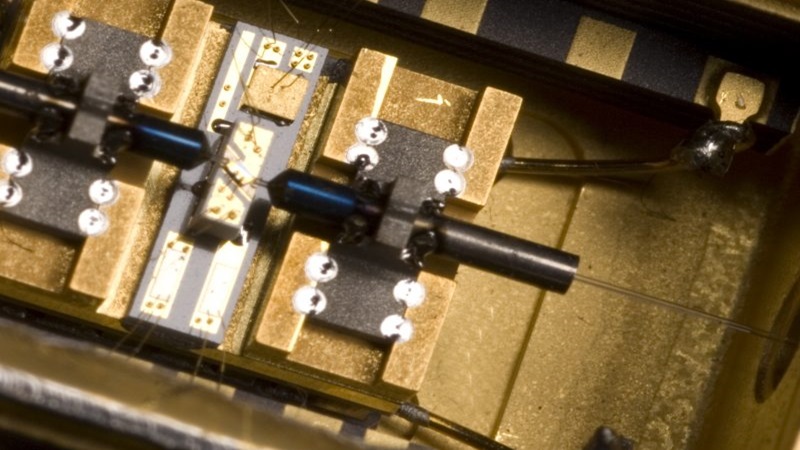
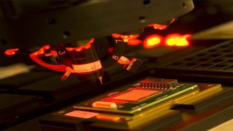
ALTER can accept customer’s wafers directly from the wafer foundry, and provide a complete back-end service including electronic wafer sort/probing, thinning and dicing, packaging and final test.
ALTER expertise and capability in wafer sawing will reduce risk and reduce time to market for your wafer saw requirements as well as providing a cost-effective manufacturing option.
Download Datasheets for advanced packaging solutions
Explore our expertise through ALTER’s Packaging and Assembly datasheets. Click now to explore cutting-edge solutions, from fast IC prototype packaging to advanced hermetic sealing. Discover our capabilities in ASIC packaging, MEMS, laser diode modules, and more.

Related services
Hermetic sealing
Plastic encapsulation
Optical Alignment
Die bonding
Flip Chip
