
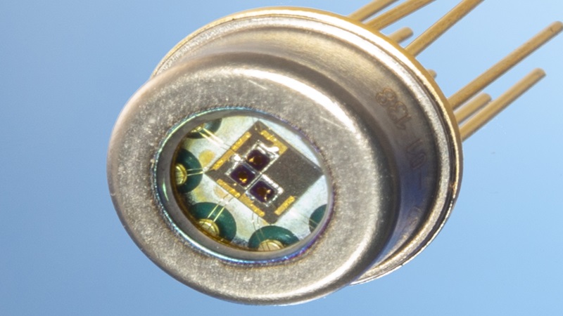
Plastic Encapsulation is a process where the semiconductor chip is assembled in a package which is directly over-moulded with an epoxy mould compound rather than being in an air cavity.

Plastic packaging offers low cost assembly with a >90% cost reduction compared to equivalent ceramic or metal packages, and enables higher volume throughput due to the nature of matrix panel assembly.
Plastic packages have been used for commercial, industrial and automotive applications for many years, and due to advancements in reliability are now being adopted for even harsh environments such as space, aerospace and defense.
ALTER has invested in the equipment and process development to make this capability accessible in Europe enabling low cost and high throughput assembly.
Plastic encapsulation fall under 3 main categories:
- Packages with external leads/pins such as DIL, SOIC, QFP and TSSOP, are based around a metal leadframe but require expensive dedicated tooling, each package requiring its mould cavity and deflash, trim, form & singulation tools. These tools are prohibitive, and ALTER has not invested in such tooling
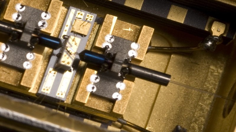
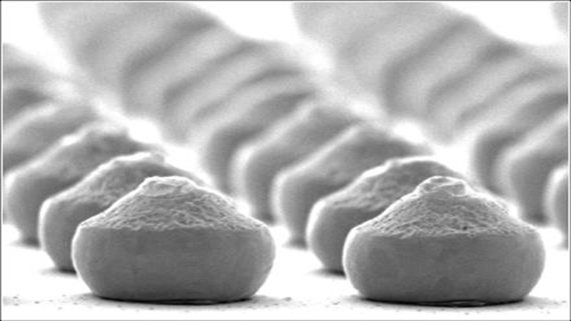
- Leadframe-based QFN (quad-flat no leads) is the core of ALTER’s current plastic package offering. QFN is a highly flexible platform using array panel tooling. An etched copper leadframe is used as the basis, which lends itself to low cost and customization. After die attach and wire bonding in array panel form, the package body is produced by over-moulding with a block mould and cut into individual packages by sawing singulation. This means that apart from the leadframe etching tool, customization is defined by machine programs rather than dedicated tooling. Contact to the PCB is through solderable NiPdAu-plated pads on the bottom surface of the QFN.
- Substrate-based ball-grid array is high on ALTER’s roadmap and can be achieved on the same moulding platform as QFN. The leadframe is replaced with a multilayer organic PCB substrate which offers high levels of complexity and interconnects.
The substrates are typically custom co-designed with the customer chip or chips. Multiple chips can be attached and connected either via the substrate connections or by direct chip to chip bonding along with passive components. This enables multi-chip modules for higher density functions. Even more complex system-in-package can be considered by incorporating different chip functions such as logic, memory, power management, connectivity and sensors into the same module. To enable these functions, different semiconductor types such as Silicon, GaN, GaAs, and novel devices such as graphene and MEMS can also be combined in the same package. This use of multiple semiconductor materials in the same module is commonly known as heterogeneous integration.
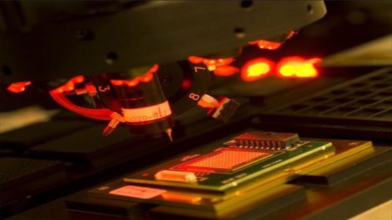
ALTER can also offer testing of plastic packaged component using state of the art high-throughput pick and place handlers in conjunction with automated test equipment.
Download Datasheets for advanced packaging solutions
Explore our expertise through ALTER’s Packaging and Assembly datasheets. Click now to explore cutting-edge solutions, from fast IC prototype packaging to advanced hermetic sealing. Discover our capabilities in ASIC packaging, MEMS, laser diode modules, and more.

Related services
Hermetic sealing
Optical alignment
Die bonding
Wafer sawing
Flip Chip
