
Packaging and Assembly for optoelectronics and microelectronic devices
ALTER is an Outsourced Semiconductor Assembly and Test (OSAT) company providing outsourced assembly/packaging and testing of microelectronic semiconductor devices such as ICs, ASICs, MEMS, sensors, laser diodes, LEDs, VCSELs and discretes.
ALTER offers a one-stop shop offering a complete back-end service for IC manufacturers, from package design, assembly and packaging, testing and qualification. This ensures all our clients’ needs and requirements can be met and minimizes the expensive capital equipment and personnel requirements of our clients.
Our expertise in semiconductor packaging solutions spans the full product life-cycle: from design through prototyping, process optimization, product qualification, failure analysis and volume manufacturing.
We offer you services in the following areas:
Fast Turn IC Packaging
Fast Turn IC prototype packaging is a service offered by ALTER that provides a rapid turnaround of prototype IC devices; if required, this can also be on a one-day basis.
Plastic encapsulation
QFN Package
Chip on Board (COB)
Package design and modelling
Hermetic Packaging
We focus our work in the following areas
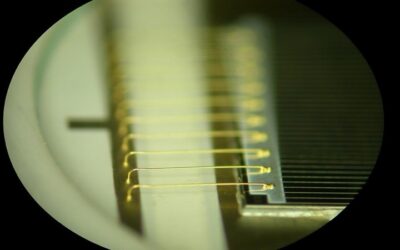
Assembly Processes
Unleashing efficiency for cost savings and swift market entry
Package Design
Providing contract package design and assembly service
Photonics Packaging
Aligning light, managing heat, ensuring excellence
Datasheets
Miniaturised Narrow Linewidth Lasers
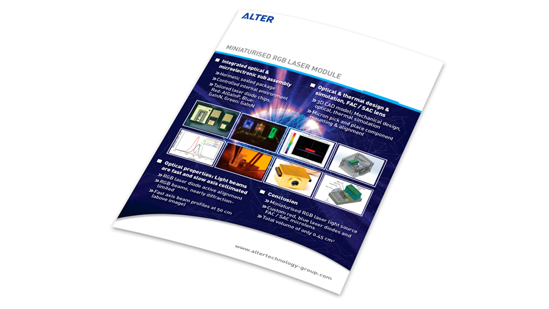
Miniaturised RGB laser module
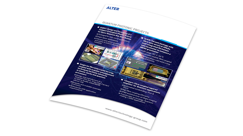
Quantum photonic projects
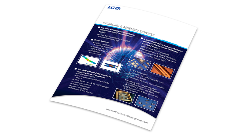
Packaging and Assembly services
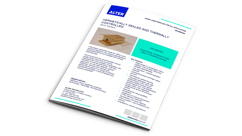
Drummond: Single Mode Collimated Diode Laser
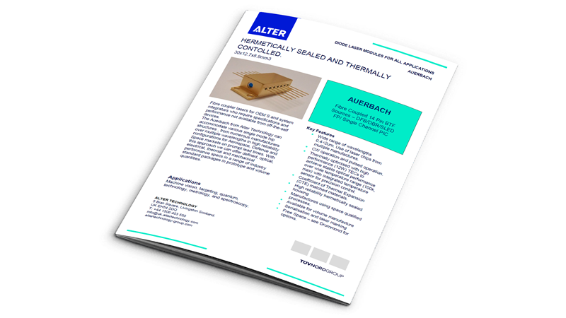
Auerbach: Fibre coupler laser
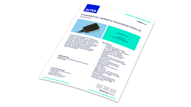
Somerville Standard PIC Packaging
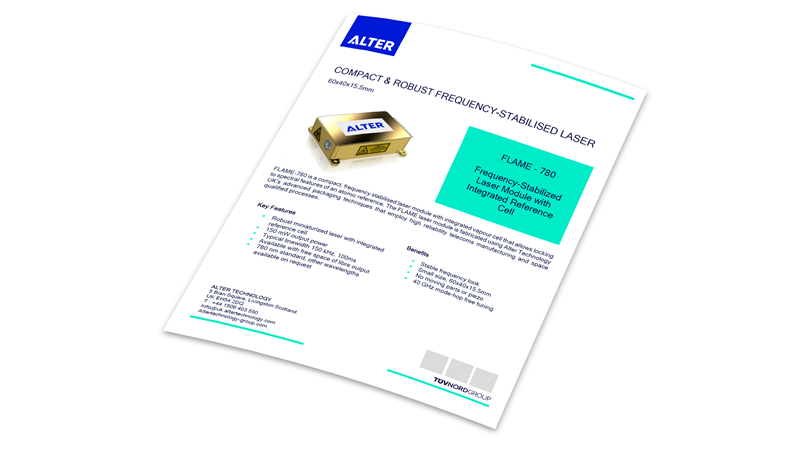
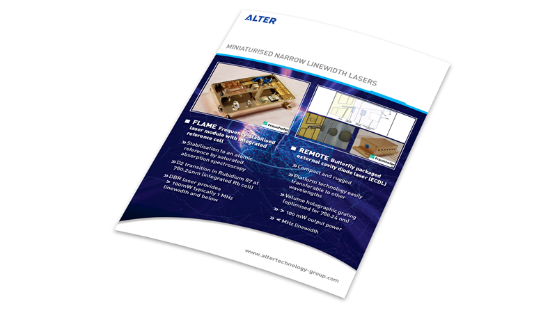
FLAME-780: Frequency Stabilised Laser
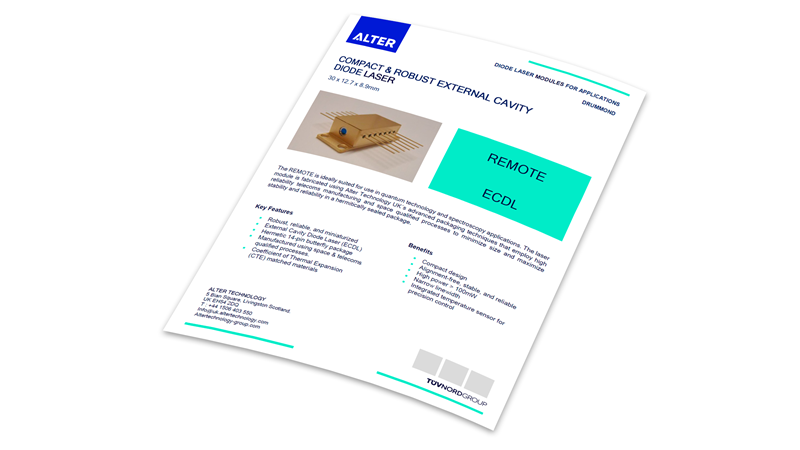
REMOTE: External Cavity Diode Laser
Current focus topics
Hermetic sealing
ALTER ensures hermetic sealing excellence for diverse metal packages, including ceramic, TO-can, and butterfly laser configurations.
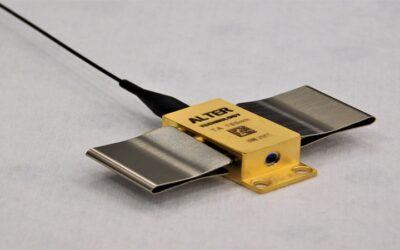
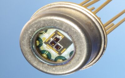
Laser diode modules
ALTER’s Laser Diode Modules: Customizable solutions, diverse configurations, and in-house assembly/testing for precision in Photonics applications.
ASIC Packaging
ASIC packaging excellence from ALTER: Fast prototype, QFN ramp-up, and volume production. Rapid validation for efficient ASIC design testing.
We support you in all packaging and assembly issues
info@uk.altertechnology.com
+44(0)1506 403 550
Contact Form
info@uk.altertechnology.com
+44(0)1506 403 550
Contact Form