
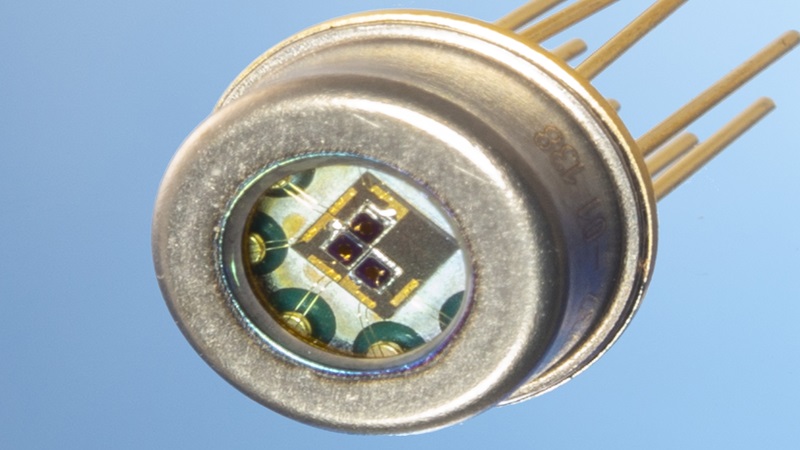
Flip chip (also known as direct chip attach) is the process whereby a semiconductor die is attached bond pad side down to a substrate or carrier.
The electrical connection is made by means of conductive bumps or balls on the die bond pad.
Flip chip bonding can offer a number of advantages over other interconnection processes. Flip chip bonding can provide higher I/O count as the whole area of the die can be used for connections. Due to the short interconnections paths, compared to wire bonds, the speed of a device can be improved. In addition, as wire bonds loops are removed it provides a smaller form factor.
ALTER can handle a range of die bumping materials including solder balls, copper pillar and gold stud bumps.

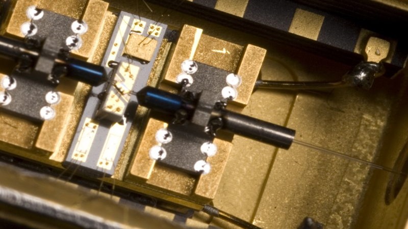
Processes for flip-chip bonding require the bumps to be melted or reflowed to form a connection between the die bond pads and the package substrate. These include thermcompression and thermosonic attach, using a combination of heat, pressure and ultrasonics, or a mass reflow approach where the die is placed on the substrate then reflow is performed off-line on a batch basis.
Wafer bumping is usually applied as a wafer-level process, however for customers not able to submit the full wafer for bumping, ALTER can provide the attach of gold stud bumps at individual die level. The Au stud bumping is achieved using a modified wire bonding process, where the 1st bond (ball) is attached to the pad, then the capillary is lifted and finally the wire is cleaved to leave the stud bump on the die’s bond pad.
Once the die is connected the stand-off distance between the die and substrate is typically filled with a non-conductive adhesive referred to as underfill. The underfill provides stress relief between the die and carrier, provides mechanical robustness, and protects the component from any moisture ingress or contamination.
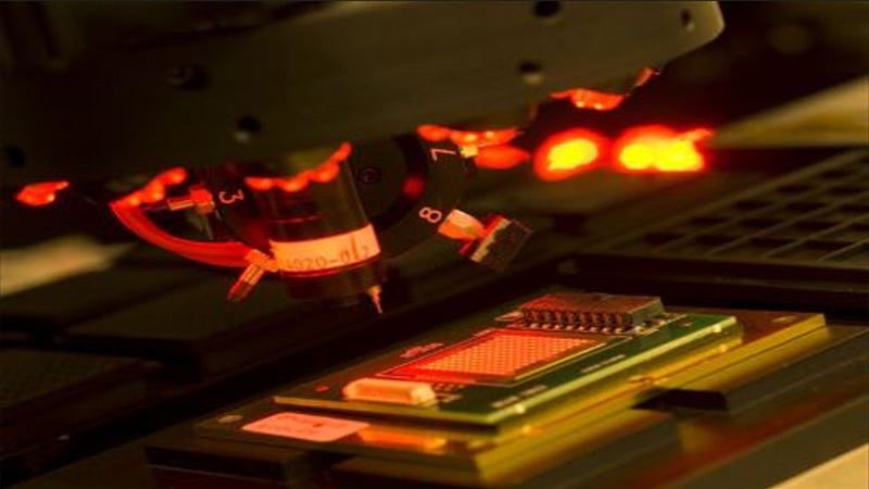
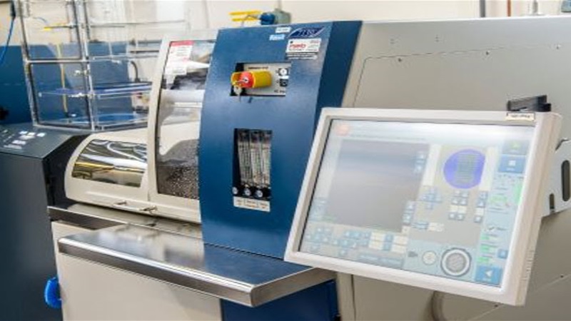
ALTER uses advanced techniques to check the quality of the flip-chip process, including our in-house micro-focus x-ray system, die shear and cross-sectioning.
Download Datasheets for advanced packaging solutions
Explore our expertise through ALTER’s Packaging and Assembly datasheets. Click now to explore cutting-edge solutions, from fast IC prototype packaging to advanced hermetic sealing. Discover our capabilities in ASIC packaging, MEMS, laser diode modules, and more.

Related services
Hermetic sealing
Plastic encapsulation
Optical alignment
Die bonding
Wafer Sawing
