We introduce cost-effective QFN plastic packaging in Scotland for mid-volume needs. Their advanced packaging platform aims at scalable volume and low-cost assembly, benefiting diverse semiconductor applications. This shift supports low to medium volume applications and early-stage high-volume product development.
Semiconductor devices are rapidly reaching the limits of what can be achieved on a single monolithic chip / die (this is signified by the apparent slowing of Moore’s Law), in addition the very advanced technology nodes used to pack more functionality onto processor chips are becoming exponentially more expensive, making them preserved for only very high specification applications.
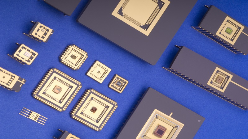
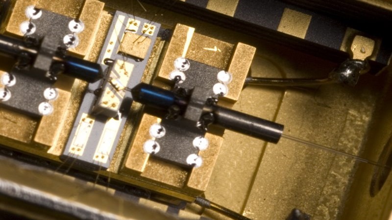
An approach to overcome these limitations is to divide the system’s functions across multiple smaller dice (or chiplets) using the most cost-effective and appropriate technology node and material. These dice are then integrated together inside a package or module in a chiplet architecture with very short and optimized interconnects, either directly between chips or by connecting the chips to advanced substrates by use of solder bumps. This level of integration cannot be achieved by using traditional circuit boards due to the large size, and impact on speed and performance. The approach of packaging multiple chips together to increase performance over traditional electronic circuit boards, is known as Advanced Packaging.
Different semiconductor materials have distinct benefits; for example, silicon (Si) is low-cost, has the most advanced manufacturing nodes and is ideal for logic and memory. Compound semiconductors offer benefits for certain applications; e.g., Gallium Nitride (GaN) is ideal for high-speed switching of voltages and radio frequencies, and Silicon Carbide (SiC) is suited to switching high currents and voltages. Novel materials such as graphene are becoming more prevalent for sensors.
An advanced packaging platform is essentially chip agnostic, meaning it can accommodate any type of semiconductor or a mixture of types in a single package. Combining multiple semiconductor platforms into a single package is known as Heterogeneous Integration, and it allows the user to leverage distinct advantages provided by each chip type and provides improved performance and functionality without continual advancements in Moore’s Law.
Until recently, Advanced Packaging has been the remit of large, overseas assembly houses, usually based in Asia. Their capacities are dominated by production for high-volume consumer, mobile, and automotive customers, which makes it difficult to support small customers. Many very relevant applications have intrinsically low and medium volumes, and even companies producing new products for high-volume applications struggle to find support during development and initial production volumes.
ALTER has started to reverse the trend by introducing low-cost QFN plastic packaging in the Scotland facility, which enables mid-volume low-cost packaging and is now developing an advanced packaging platform that will provide scalable volume and low-cost assembly compatible for end users, chip designers, wafer fabs, and foundries across multiple die technology types.
Related services
Hermetic Packaging
QFN Package