- Stacking MEMS, ASICs and interposers
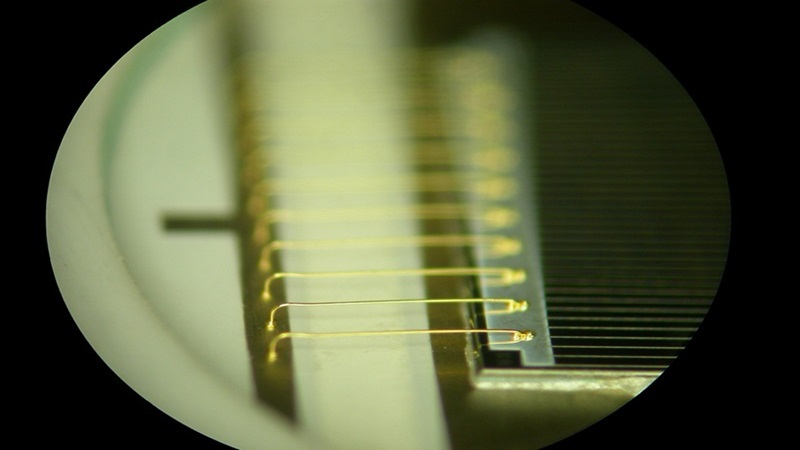
- Die-to-die wire bonding
- Handling of sensitive membrane die
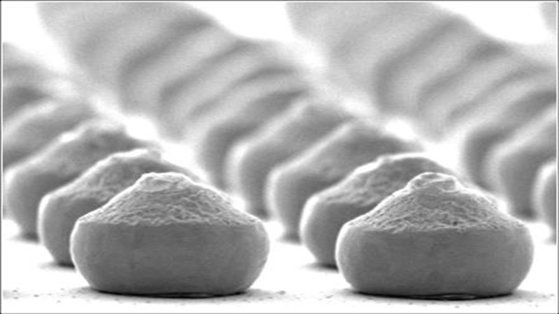
- Low-stress adhesives
- Open tools or custom packages
- Over-molded plastic packages (QFN)
- Cavity metal, ceramic or plastic packages
- Hermetic and Vacuum sealing

MEMS devices packaging and assembly: ALTER's key expertise
ALTER has experience in the assembly and packaging of microelectromechanical system (MEMS) devices such as inertial sensors, accelerometers, microfluidic devices and optical MEMS.
ALTER offers customers support in prototype/process development for MEMS packaging and volume manufacturing capability. By prototyping on the volume manufacturing toolset, ALTER can offer a risk-free transition to manufacturing with a fully optimised and high-yield process.
There are a number of specific technical challenges related to MEMS assemblies such as special handling techniques to avoid damage to sensitive chip structures and the use of specialist adhesives and materials to avoid inducing stresses in the MEMS die.
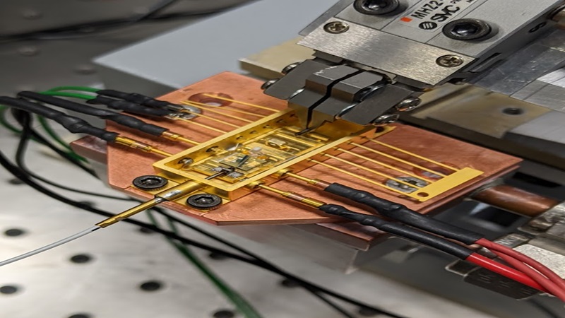
As a result, ALTER has developed an extensive “tool-kit” of material and process knowledge in all key steps of the assembly process, including wafer saw, die-attach, flip-chip attach, wire bonding, and encapsulation. This tool kit of process and material knowledge is used to reduce development times and reduce development and manufacturing risks for customers.
Advanced packaging techniques such as die stacking, and die wire bonding can also be used to integrate MEMS die with other chips such as controllers and ASICs as a System-in-Package (SiP) and support the increasing trends in miniaturization and lower costs.
Important parameters for the washing step include wash time, wash rpm, DI water pressure, dry time, dry rpm, temperature and airflow rate. As a company, we have developed a number of optimized wafer saw and wash processes for various MEMS and sensor devices in order to avoid damage to the sensitive membrane and optical surfaces.
ALTER can accept customer’s wafers directly from the wafer foundry, and provide a complete back-end service including electronic wafer sort/probing, thinning and dicing, packaging and final test.
ALTER expertise and capability in wafer sawing will reduce risk and reduce time to market for your wafer saw requirements as well as providing a cost-effective manufacturing option.
Download Datasheets for advanced packaging solutions
Explore our expertise through ALTER’s Packaging and Assembly datasheets. Click now to explore cutting-edge solutions, from fast IC prototype packaging to advanced hermetic sealing. Discover our capabilities in ASIC packaging, MEMS, laser diode modules, and more.

Related services
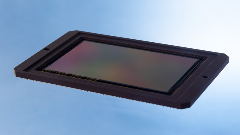
Image sensor packaging
Chip on board
System in package