Image sensor packaging presents a unique set of challenges to ensure the correct function, integrity and function of the device, not usually considered with standard microelectronic components.
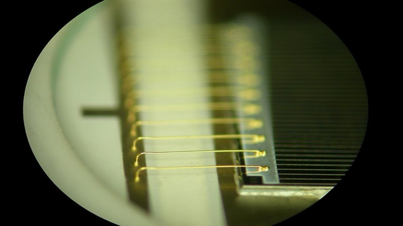
Optical devices need to be handled sensitively to ensure no contact with the sensor area and without introducing particles which would impact the optical function of the sensor. The position and tilt of the sensor within the package can be critical when integrating with further optics in camera systems, and packaging should be defined in such a way as to avoid stray light coming into the sensor.

Off-the-shelf microelectronic packages for ASICs tend to have small and square cavities, which are not a close fit for large sensor dies. A chip-on-board approach can sometimes be combined with our dam & process to encapsulate the wire bonds and die edge, exposing the sensor area.
For customers wanting to enclose the sensor in a sealed or hermetic package, ALTER offers bespoke package and window lid design services.
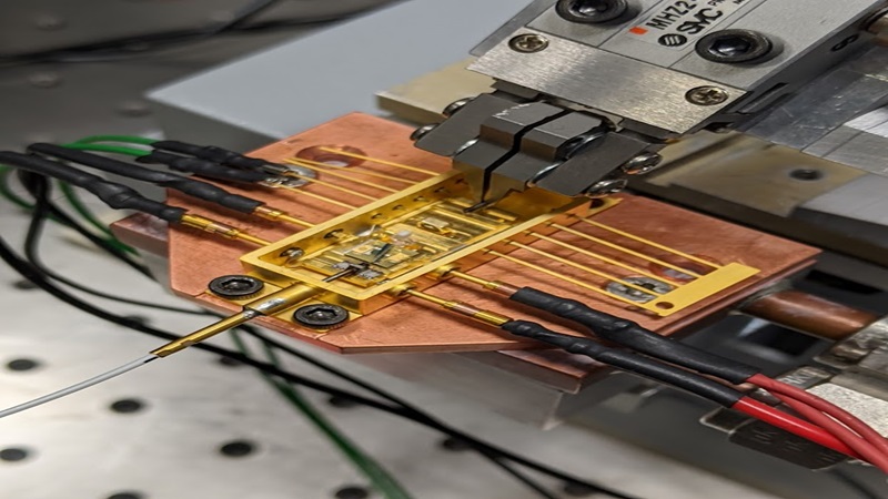
Sensors are handled with our automated assembly equipment, ensuring a hands-off approach, reducing contamination and ensuring high placement accuracy and consistency tolerances. Sub-micron metrology is used during set-up to measure and ensure placement and can also be used for quality checks on 100% of the devices if requested.
Dedicated pick-up tools are usually used to avoid the sensor’s optical area entirely. This use of automated equipment also enables high throughput and volume assembly.
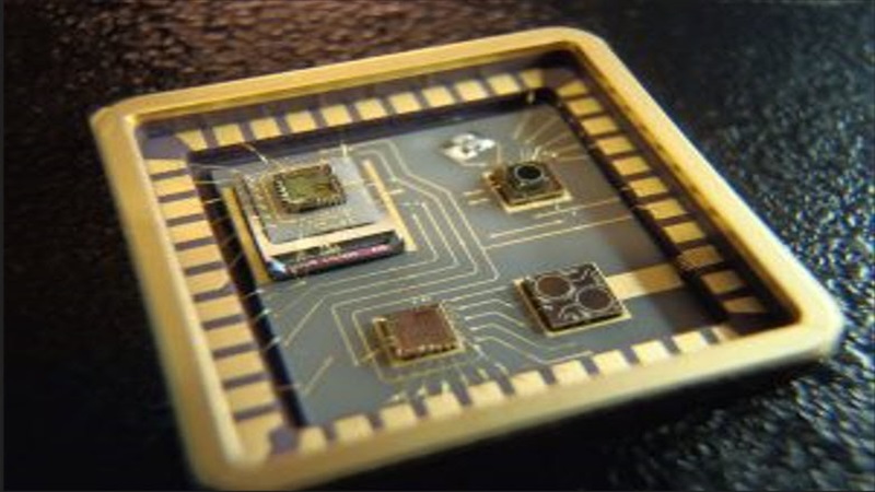
Specialist cleaning procedures can be employed to remove any remaining particles prior to the final lid attach and sealing. ALTER can combine image sensor packaging with integrated thermoelectric coolers and seal with an internal vacuum for applications such as infrared imagers to reduce background thermal interference. ALTER has produced image sensors for volume applications such as machine vision and challenging applications, including deep-space exploration.
Our specialist Optoelectronics testing laboratory in Madrid can provide image sensor characterisation and qualification as a part of their applications services.
Assembly Capabilities
- Optimised wafer saw processes.
- Precision placement
- Filter and glass placement
- Specialist particle control
- Black dam & aperture attach
- Hermetic Sealing
- Chip-on-board
Image sensor packaging process Highlights
- Automated Die placement accuracy +/-15µm
- Rotation control 2° to 5°, tilt control <50µm
- Programmable epoxy dispensing pattern
- Thermal or UV snap cure to maintain die position
- Controlled clean environments – ISO7 cleanroom & laminar flow (ISO5)
- CO2 cleaning optimised for sensor and glass.
- Hermetic seam sealing in an inert N2 environment
- <5000ppm moisture content
- Black dam dispensing for stray light
Download Datasheets for advanced packaging solutions
Explore our expertise through ALTER’s Packaging and Assembly datasheets. Click now to explore cutting-edge solutions, from fast IC prototype packaging to advanced hermetic sealing. Discover our capabilities in ASIC packaging, MEMS, laser diode modules, and more.

Related services
Chip on board
MEMS Packaging
System in package