Optoelectronic or Photonic packaging requires extremely accurate placement of components to ensure appropriate alignment and coupling of light into and out of devices.
In many cases the generation or detection of light results in significant heat being generated, which if not suitably dissipated through appropriate joining technology and material selection, can adversely affect the device operation. Additionally, assembly processes can be complicated by the requirement that fluxes and many other organic materials can’t be used as they can degrade the performance of facets in optical devices.
A key function of an optoelectronic device is to manipulate light. As a result, the packaging and assembly processes for many optoelectronic components can be significantly more complex than traditional microelectronic devices.
ALTER has experience in the assembly and packaging of a wide range of Optoelectronic devices, including:
- High-power laser diodes
- PV Cells
- Optical Interconnects
- DFB’s, SOA’s
- Mach-Zender Interferometers
- Modulators
- Photodetectors
- TOSA/ROSA’s
ALTER UK expertise and capability in Photonic Packaging will reduce risk, reduce time to market for your Optoelectronic packaging requirements, and provide a cost-effective manufacturing option.
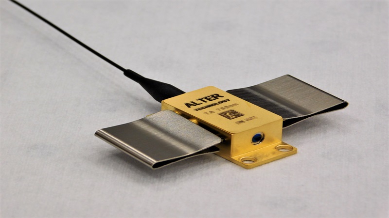
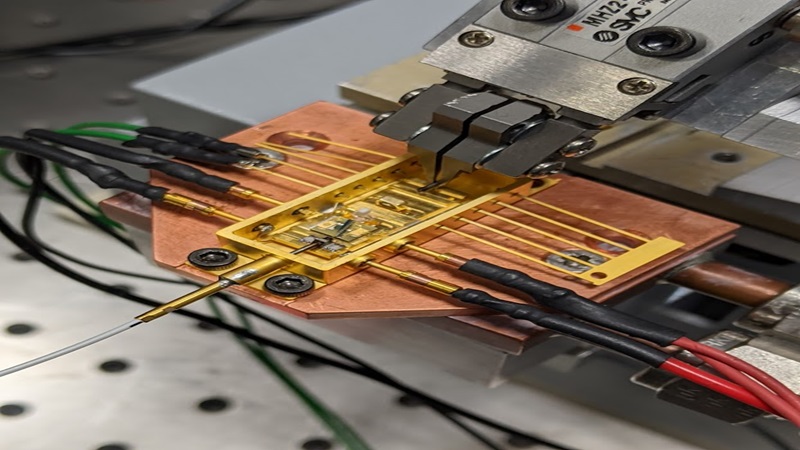
Laser Diode Packaging
ALTER offers customers support in both prototype/process development for laser diode packaging as well as volume manufacturing capability.
By prototyping on the volume manufacturing tool-set ALTER can offer a risk-free transition to manufacturing with a fully optimised and high yield process.
A summary of ALTER laser diode packaging expertise can be found below:

Process Highlights
- Placement accuracies from +/- 1µm to +/-20µm
- Fully automated or manual placement
- Adjustable band force
- 3-axis placement control
- Void-free Eutectic die attach
- Control of flatness “smile”
- Epi-side down or up assembly
- Vacuum reflow processes
Materials
- GaAs or InP
- Size
- Laser bars over 10mm
- Laser single emitters to 5mm
Package Type
- C-mount (standard sizes of 4mm to 5mm, sharp edge for accurate placement)
- CS-mount
- TO-can
- Stacks
Eutectic solder processes including AuSn, SnAg, InAg, SnPb, BiSn (preforms, pre-deposited substrates to control solder overspill
CuW/Cu/AlN/CuW/CVD Diamond sub-mounts and heat-sinks
ALTER expertise and capability in Laser Diode Packaging will reduce risk and reduce time to market for your laser diode packaging requirements as well as providing a cost-effective manufacturing option.
Fiber Alignment

ALTER offers a standard Telcordia-compliant platform for packaging and fibre coupling optoelectronic devices into a 14-pin Butterfly package. This standard platform incorporates a Thermistor, Thermoelectric Cooler (TEC) and back-facet photodiode monitor. A full flux and organic-free process are used to avoid contamination that may compromise the delicate optical surfaces. A fully hermetic seal casing in an inert gas atmosphere offers an increased lifetime of the optoelectronic device. A laser-welded fibre attach process provides a robust and reliable attachment. This standard platform has undergone extensive environmental testing for demanding Telcordia standards.
ALTER UK, the standard platform provides several key benefits:
- Avoids Design and Development NRE charges.
- Utilises Telcordia/Space compliant processes and materials.
- Enables faster time to market by utilising off-the-shelf components and avoiding key technical pitfalls.
- Provides competitive unit prices based on automated assembly processes and utilising economies of scales for purchasing materials.
ALTER UK, the standard platform has the following features:
- Wide range of packages including 14-pin butterfly packages and TO-cans.
- PM, SM, MM, Polycrystalline, High-temperature fibres and FVA’s including lensed options.
- Laser weld or epoxy attach of fiber assembly
- High-quality AR coating with a variety of lens designs to maximise coupling efficiency
- Solutions for a wide range of devices and wavelengths including DFB, DBR lasers, SOA’s, SLD’s VCSEL’s, Photodiodes and Quantum Cascade lasers
- Isolators and Free-Space optics
- Thermistor, TEC and Monitor Photodiode
Download datasheets for advanced packaging solutions
Explore our expertise through ALTER’s Packaging and Assembly datasheets. Click now to explore cutting-edge solutions, from fast IC prototype packaging to advanced hermetic sealing. Discover our capabilities in ASIC packaging, MEMS, laser diode modules, and more.


Related services
Photonic Integrated Circuit (PIC)