
LED Chip-on-Board benefits and advantages: cost-effectiveness, custom arrays, enhanced efficiency, and reduced ownership costs.
Why LED Chip-on-Board?
Cost-effective alternative to incandescent and fluorescent light sources
- Increased life span and efficiency
- System integration, no user-serviceable parts
- The reduced total cost of ownership
- Customised array size and shape
- Application-specific wavelengths
Chip-on-board vs. surface-mounted LEDs:
- Low-pitch / higher density arrays
- Improved efficiency and heat dissipation
- No over-moulding material boosts light output
- Fewer interconnects reduce reliability risk

Why ALTER?
Value Proposition
- Experienced LED CoB module provider
- The flexible and customisable platform
- Reduced time to market:
- Product-specific experience and processes
- Established material supply chain
- Reduced technical risk
- Existing design and process knowledge
- Rapid prototyping on production tools
- Reduced cost
- There is no capex requirement for the customer Volume manufacturing capacity
- >200K LED placements per month.
Concept to a product:
- Substrate design & sourcing, ceramic, IMS, FR4.
- Sourcing tested & binned LED dies
- Optical and thermal modelling
- Full range of volume assembly services
- Functional test
- Characterisation
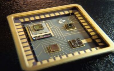
Assembly Capabilities
Die Attach
- Ag epoxy stamping or dispensing
- Sintering epoxy materials
- Soldering
- Pick from film/frame, waffle or gel pack.
- Flip-chip attach & Au stud bumping
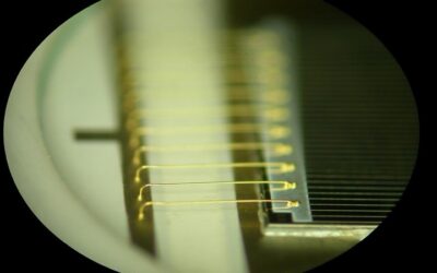
Wire Bond
- 17 to 50um Au ball bonding
- Plasma clean for improved adhesion
- Encapsulation Options
- Frame laser cutting and attach
- Glass cover attach
- Silicone encapsulation
- Dome attach
- Specialist processes for mixing and degassing
QC checks
- Die shear and wire strength tests
- Placement accuracy measurements
Important parameters for the washing step include wash time, wash rpm, DI water pressure, dry time, dry rpm, temperature and airflow rate. As a company, we have developed a number of optimized wafer saw and wash processes for various MEMS and Sensor devices in order to avoid damage to the sensitive membrane and optical surfaces.
ALTER can accept customer’s wafers directly from the wafer foundry, and provide a complete back-end service including electronic wafer sort/probing, thinning and dicing, packaging and final test.
ALTER expertise and capability in wafer sawing will reduce risk and reduce time to market for your wafer saw requirements as well as providing a cost-effective manufacturing option.
Download Datasheets for advanced packaging solutions
Explore our expertise through ALTER’s Packaging and Assembly datasheets. Click now to explore cutting-edge solutions, from fast IC prototype packaging to advanced hermetic sealing. Discover our capabilities in ASIC packaging, MEMS, laser diode modules, and more.


Related Blog
ASIC Packaging
ASIC packaging excellence from ALTER: Fast prototype, QFN ramp-up, and volume production. Rapid validation for efficient ASIC design testing.
MEMS Packaging
ALTER excels in MEMS packaging, precision assembly of inertial sensors, accelerometers, microfluidic, and optical MEMS devices.
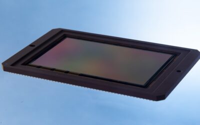
Image sensor packaging
Explore ALTER UK’s expertise in image sensor packaging assembly. Overcome unique challenges for correct function and device integrity.