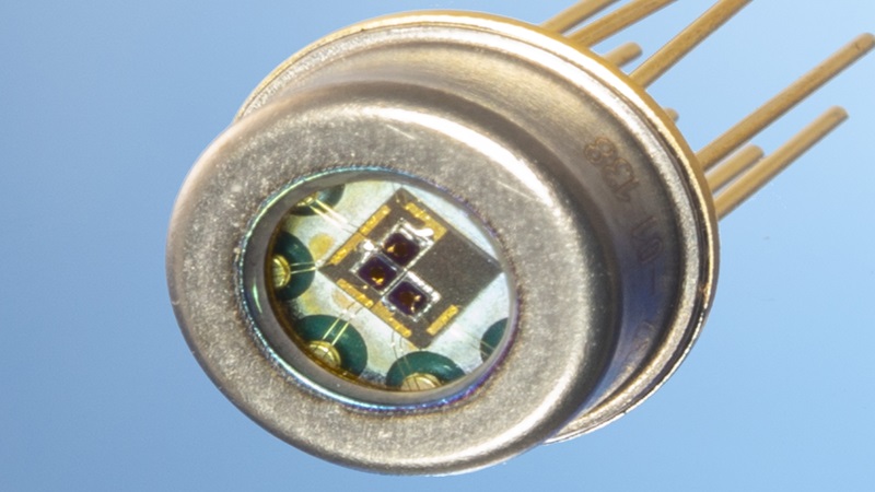
ALTER ensures hermetic sealing excellence for diverse metal packages, including ceramic, TO-can, and butterfly laser configurations.
Hermetic sealing
read more

ALTER ensures hermetic sealing excellence for diverse metal packages, including ceramic, TO-can, and butterfly laser configurations.
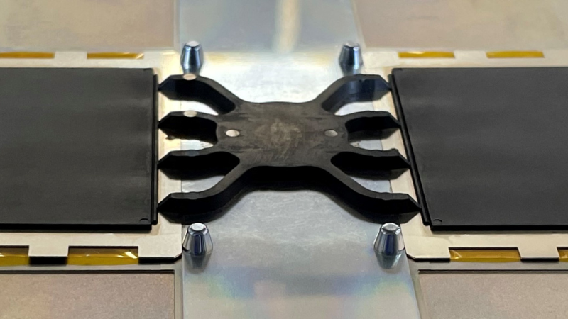
Plastic encapsulation molds semiconductor chips directly with epoxy, avoiding air cavities. A streamlined process for chip assembly in packaging.
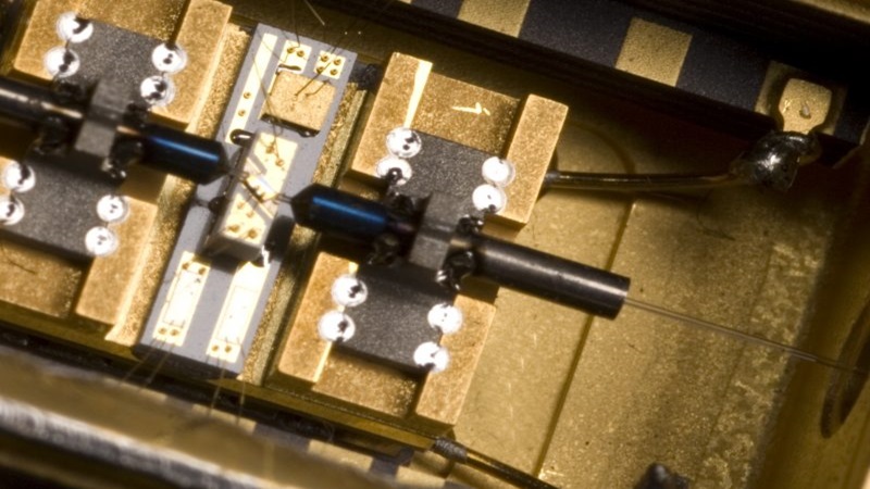
ALTER specializes in optical alignment, aligning optical fibers and components to various optoelectronic devices like diode lasers and Photonics ICs.
Die bonding in semiconductor assembly ensures robustness, electrical connectivity, and effective heat removal, considering thermal, electrical, and mechanical factors.
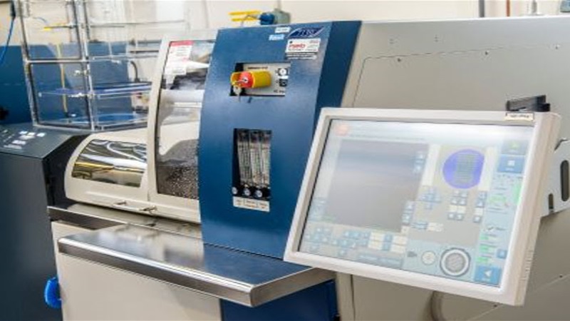
ALTER excels in wafer sawing, singulating wafers up to 12” for precise assembly in Plastic package and System-in-Package (SiP) applications.
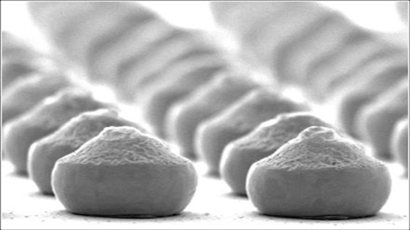
Explore flip chip efficiency in semiconductor assembly. ALTER excels in precise, bond pad-down attachment for superior electrical connections.
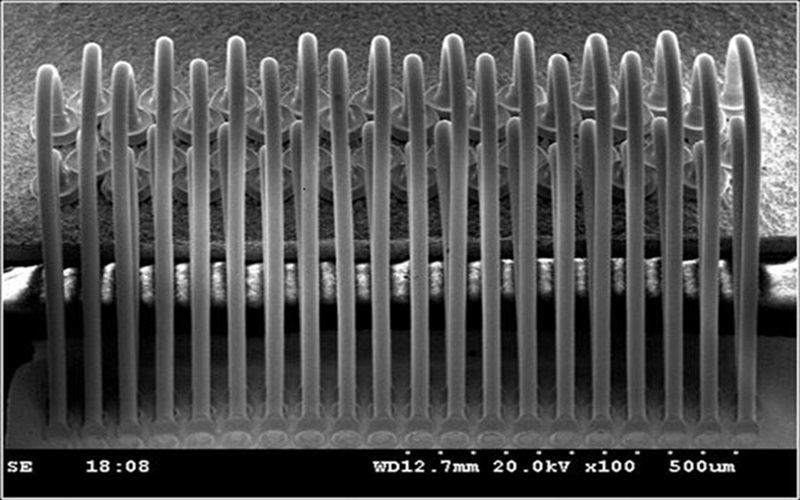
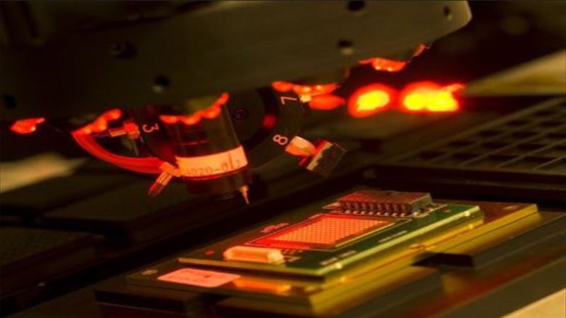
Explore wire bonding in semiconductor packaging. ALTER ensures optimal processes through collaborative design, maximizing yield.
ALTER ensures hermetic sealing excellence for diverse metal packages, including ceramic, TO-can, and butterfly laser configurations.
Plastic encapsulation molds semiconductor chips directly with epoxy, avoiding air cavities. A streamlined process for chip assembly in packaging.
ALTER specializes in optical alignment, aligning optical fibers and components to various optoelectronic devices like diode lasers and Photonics ICs.
Die bonding in semiconductor assembly ensures robustness, electrical connectivity, and effective heat removal, considering thermal, electrical, and mechanical factors.
ALTER excels in wafer sawing, singulating wafers up to 12” for precise assembly in Plastic package and System-in-Package (SiP) applications.
Explore flip chip efficiency in semiconductor assembly. ALTER excels in precise, bond pad-down attachment for superior electrical connections.
Explore wire bonding in semiconductor packaging. ALTER ensures optimal processes through collaborative design, maximizing yield.