ALTER excels in assembling and packaging Photonic Integrated Circuit (PIC) devices, including Silicon and InP PIC. Expert PIC packaging for optimal performance.
Photonic Integrated Circuit (PIC) Packaging
read more

Home >
ALTER excels in assembling and packaging Photonic Integrated Circuit (PIC) devices, including Silicon and InP PIC. Expert PIC packaging for optimal performance.
12” / 300mm wafer dicing is now available at ALTER UK, enhancing support for the European semiconductor industry.
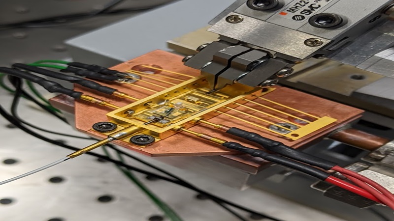
ALTER UK is developing a Co-Packaged Optical Transceiver for space, enhancing satellite communication with photonic and microelectronics integration.
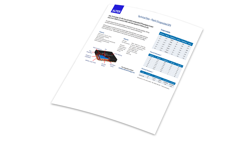
ALTER UK offers low-cost plastic encapsulated QFN packaging for batch sizes from 100pcs to several 1000s, with total capacity for millions per year.
ALTER UK is developing a Co-Packaged Optical Transceiver for space, enhancing satellite communication with photonic and microelectronics integration.
ALTER UK offers low-cost plastic encapsulated QFN packaging for batch sizes from 100pcs to several 1000s, with total capacity for millions per year.
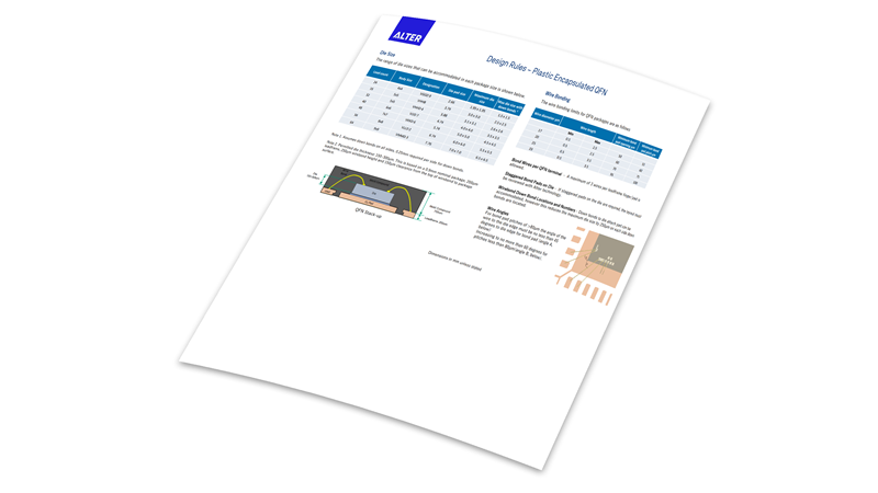
Explore ALTER’s plastic encapsulated QFN design rules for precise and reliable packaging solutions. Optimize your semiconductor performance.
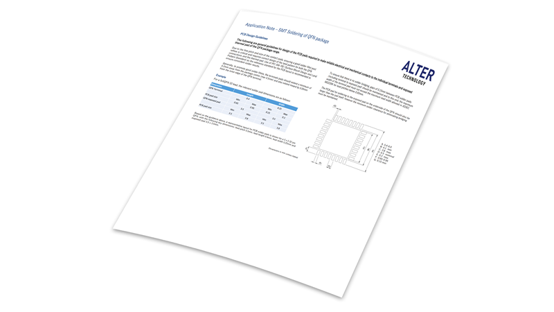
This factsheet contains general guidelines for design of the PCB pads required to make reliable electrical and mechanical contacts to the individual terminals and exposed thermal pad of the QFN package range.
Unlock the potential of our Packaging and Assembly expertise.
Click now to access valuable resources and elevate your semiconductor solutions with ALTER.

Downloads 25 KB | PDF
ALTER UK offers low-cost plastic encapsulated QFN packaging for batch sizes from 100pcs to several 1000s, with total capacity for millions per year.
Explore ALTER’s plastic encapsulated QFN design rules for precise and reliable packaging solutions. Optimize your semiconductor performance.
Plastic encapsulation molds semiconductor chips directly with epoxy, avoiding air cavities. A streamlined process for chip assembly in packaging.
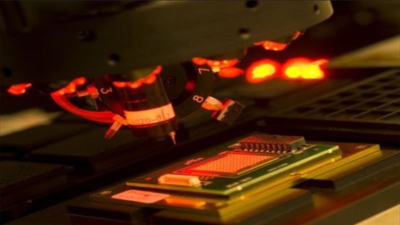
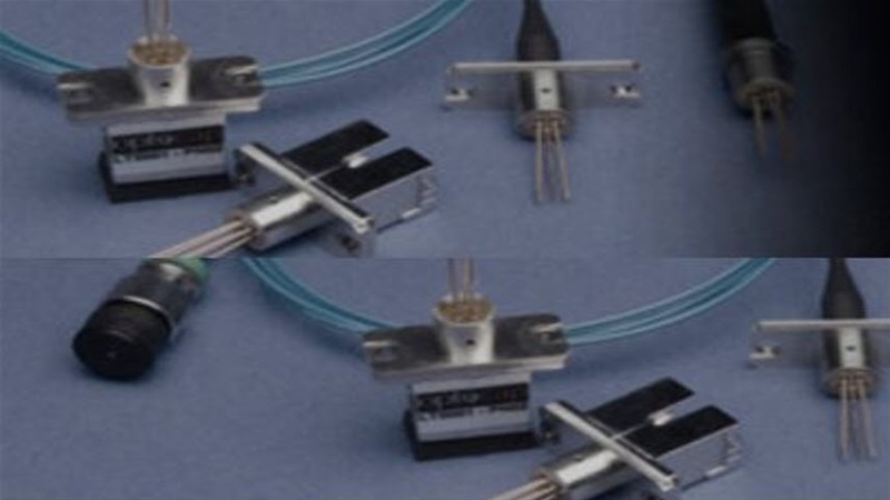
ALTER specializes in optical alignment, aligning optical fibers and components to various optoelectronic devices like diode lasers and Photonics ICs.
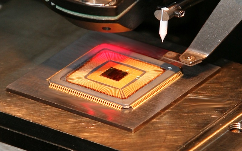
Die bonding in semiconductor assembly ensures robustness, electrical connectivity, and effective heat removal, considering thermal, electrical, and mechanical factors.
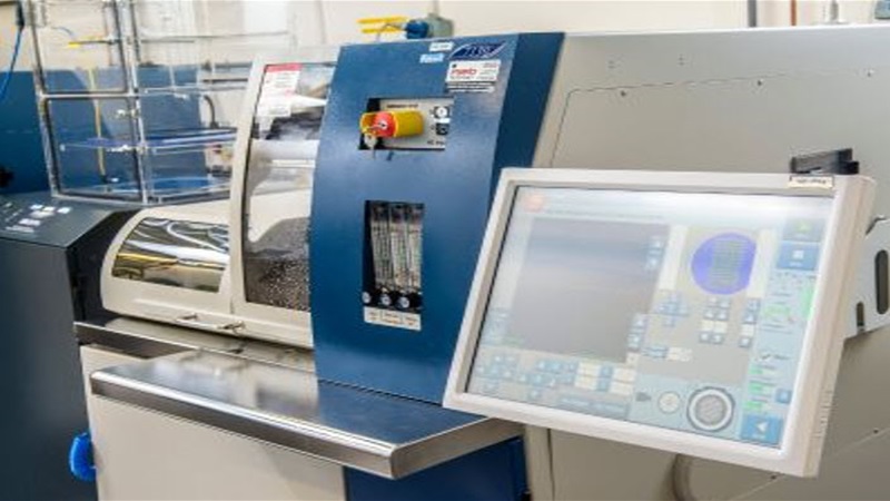
ALTER excels in wafer sawing, singulating wafers up to 12” for precise assembly in Plastic package and System-in-Package (SiP) applications.
ALTER excels in assembling and packaging Photonic Integrated Circuit (PIC) devices, including Silicon and InP PIC. Expert PIC packaging for optimal performance.
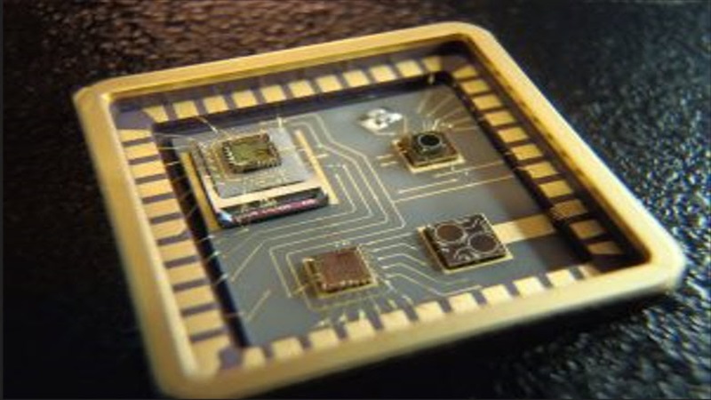
ALTER excels in MEMS packaging, precision assembly of inertial sensors, accelerometers, microfluidic, and optical MEMS devices.
LED Chip-on-Board benefits and advantages: cost-effectiveness, custom arrays, enhanced efficiency, and reduced ownership costs.
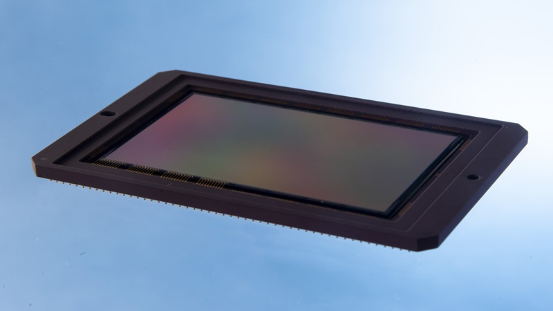
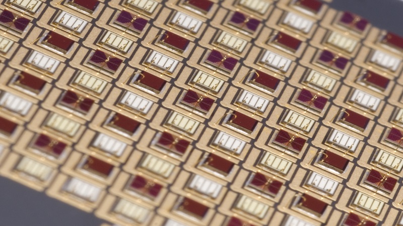
Explore ALTER UK’s expertise in image sensor packaging assembly. Overcome unique challenges for correct function and device integrity.
Precision in Optoelectronic or Photonic Packaging ensures accurate alignment and coupling of light into and out of devices.
ALTER UK offers customers support in both prototype/process development for RF Module Packaging as well as volume manufacturing capability.
This factsheet contains general guidelines for design of the PCB pads required to make reliable electrical and mechanical contacts to the individual terminals and exposed thermal pad of the QFN package range.
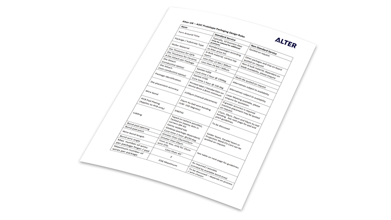
This ALTER’s factsheet introduces ASIC Prototype Packaging Design Rules and Non-standard wire/pad guidelines.
12” / 300mm wafer dicing is now available at ALTER UK, enhancing support for the European semiconductor industry.
ALTER UK is developing a Co-Packaged Optical Transceiver for space, enhancing satellite communication with photonic and microelectronics integration.
ALTER UK offers low-cost plastic encapsulated QFN packaging for batch sizes from 100pcs to several 1000s, with total capacity for millions per year.
ALTER UK offers low-cost plastic encapsulated QFN packaging for batch sizes from 100pcs to several 1000s, with total capacity for millions per year.
Explore ALTER’s plastic encapsulated QFN design rules for precise and reliable packaging solutions. Optimize your semiconductor performance.
12” / 300mm wafer dicing is now available at ALTER UK, enhancing support for the European semiconductor industry.
ALTER UK is developing a Co-Packaged Optical Transceiver for space, enhancing satellite communication with photonic and microelectronics integration.
ALTER UK offers low-cost plastic encapsulated QFN packaging for batch sizes from 100pcs to several 1000s, with total capacity for millions per year.
Unlock the potential of our Packaging and Assembly expertise.
Click now to access valuable resources and elevate your semiconductor solutions with ALTER.
Download 25 KB | PDF
Plastic encapsulation molds semiconductor chips directly with epoxy, avoiding air cavities. A streamlined process for chip assembly in packaging.
ALTER specializes in optical alignment, aligning optical fibers and components to various optoelectronic devices like diode lasers and Photonics ICs.
Die bonding in semiconductor assembly ensures robustness, electrical connectivity, and effective heat removal, considering thermal, electrical, and mechanical factors.
ALTER excels in wafer sawing, singulating wafers up to 12” for precise assembly in Plastic package and System-in-Package (SiP) applications.
ALTER excels in assembling and packaging Photonic Integrated Circuit (PIC) devices, including Silicon and InP PIC. Expert PIC packaging for optimal performance.
ALTER excels in MEMS packaging, precision assembly of inertial sensors, accelerometers, microfluidic, and optical MEMS devices.
LED Chip-on-Board benefits and advantages: cost-effectiveness, custom arrays, enhanced efficiency, and reduced ownership costs.
Explore ALTER UK’s expertise in image sensor packaging assembly. Overcome unique challenges for correct function and device integrity.
Precision in Optoelectronic or Photonic Packaging ensures accurate alignment and coupling of light into and out of devices.
ALTER UK offers customers support in both prototype/process development for RF Module Packaging as well as volume manufacturing capability.
This factsheet contains general guidelines for design of the PCB pads required to make reliable electrical and mechanical contacts to the individual terminals and exposed thermal pad of the QFN package range.
This ALTER’s factsheet introduces ASIC Prototype Packaging Design Rules and Non-standard wire/pad guidelines.